High-K oxides for new generations of transistors
The miniaturization of semiconductor components has lead to structures on the nano-scale. Further scaling is limited because the smallest structures approach atomic dimensions. In order to make further progress, new materials are required.
 The basic element of logic operations is the
transistor, which is basically a simple switch. The technological
progress rests on scaling down all dimensions of the
transistor. Smaller size means higher clock frequency, less power
consumption, and cheaper production. The smallest structure in the
transistor is the so-called gate dielectric or gate oxide, an
electrically insulating layer, which has to withstand enormous
electric fields. Currently, the thickness of the gate oxide is about
one nanometer, corresponding to about five atoms stacked ontop of each
other. If this gate dielectric is made even thinner, as required by
the scaling laws that govern miniaturization, it will loose its
insulating properties and thus will not do its function.
The basic element of logic operations is the
transistor, which is basically a simple switch. The technological
progress rests on scaling down all dimensions of the
transistor. Smaller size means higher clock frequency, less power
consumption, and cheaper production. The smallest structure in the
transistor is the so-called gate dielectric or gate oxide, an
electrically insulating layer, which has to withstand enormous
electric fields. Currently, the thickness of the gate oxide is about
one nanometer, corresponding to about five atoms stacked ontop of each
other. If this gate dielectric is made even thinner, as required by
the scaling laws that govern miniaturization, it will loose its
insulating properties and thus will not do its function.
The suggested remedy is to replace silicon dioxide, the current gate oxide material, by so-called high-k oxides, that can be used with a larger physical thickness. In the future, these high-k oxides need to be integrated with an epitaxial (atomically well-defined) interface to silicon, which poses a major challenge. We investigate the deposition of these oxides with first-principles electronic structure and ab-initio molecular dyanmics simulations in order to unravel the growth process and thus to provide the experimentalists valuable hints on the choice of materials and growth conditions.
We systematically investigated the three relevant rows in the periodic table, namely di-valent, tri-valent and four-valent metals. The four-valent Zr tends to form silicides, which is detrimental to layer-by-layer growth. Divalent metals such as Sr, on the other hand seem to be well suited. They prefer to form oxides before silicon oxidizes and rthey do not immediately form silicides.
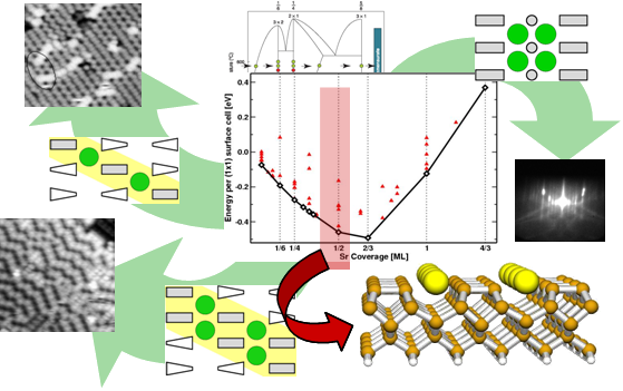 The main part of the research was to study the growth
of SrTiO3 on silicon. Researchers from the Oak-Ridge National
Laboratory have shown that epitaxial, that is atomically defined
layer-by-layer growth, of this material on silicon was
possible. However, there have beed questions regarding the atomic
structure and the relevant chemical processes during growth.
The main part of the research was to study the growth
of SrTiO3 on silicon. Researchers from the Oak-Ridge National
Laboratory have shown that epitaxial, that is atomically defined
layer-by-layer growth, of this material on silicon was
possible. However, there have beed questions regarding the atomic
structure and the relevant chemical processes during growth.
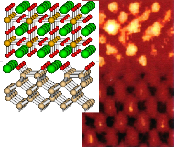 With ab-initio simulations we simulated all the
relevant processes during growth and linked our results to the
available experimental data. As a result a new model for the atomic
structure and composition of the interface emerged than what has
previously believed.
With ab-initio simulations we simulated all the
relevant processes during growth and linked our results to the
available experimental data. As a result a new model for the atomic
structure and composition of the interface emerged than what has
previously believed.
While the interface of SrTiO3 and silicon had the desirable atomic structure its electronic structure has been known to be dissatisfactory. Electrons that should pass the transistor within the silicon channel would escape through the gate oxide, because the injection barrier was too low. Our simulations also showed a possible path to improve the electrical properties. By oxidizing the interface a microscopic electrical dipole would be created that increases the injection barrier into the desired range. If verified experimentally, this would be one of the first verifications for successful band gap engineering by chemical reactions.
For further details see
- "The interface between silicon and a high-k oxide",
C.J. Först, C.R. Ashman, K. Schwarz and P.E. Blöchl, Nature 427, 53 (2004) - "Chemistry of La on the Si(001) surface from first principles",
C.R. Ashman, C.J. Först, K. Schwarz and Peter E. Blöchl, Phys. Rev. B., 70,155330 (2004) - "First-Principles Calculations of Strontium on Si(001)",
C.R. Ashman, C.J. Först, K. Schwarz and P.E. Blöchl, Phys. Rev. B 69, 75309 (2004) - "Heteroepitaxial Growth of High-K Oxides: Insights from
first-principles calculations on Zr on Si(001)",
C.J. Först, P.E. Blöchl and K.Schwarz, Comp. Mater. Sci. 27, 70-74 (2003) - "Struktur, insbesondere Halbleiterstruktur, sowie Verfahren zur
Herstellung einer Struktur",
C.J. Först, C.R. Ashman and P.E. Blöchl, German Patent, Aktenzeichen 103 03 875 from Jan. 22, 2005. - "The interface between the high-k oxide LaAlO3 and
Si(001)",
C.J. Först, K. Schwarz and P.E. Blöchl, Phys. Rev. Lett. 95, 137602 (2005) - "Ab-initio simulations on growth and interface properties of
epitaxial high-k oxides on silicon",
C.J. Först, C.R. Ashman, K. Schwarz and P.E. Blöchl, Microelectronic Engineering, 80, 402 (2005).