Defect chemistry in silica-based oxides
Oxides are the second most important class of materials for information technology, following semiconductors. The success of silicon as semiconductor of choice is based on the quality of its native oxide, silica (SiO2). Silica, which is known as inert and stable material, unfolds an amazing complexity in its defect structure, which dominates many of its properties.Silica is is important in a number of technologically important areas:
 Silica is a key component of current transistors,
metal-oxide-semiconductor field effect transistors
(MOSFETS). The ongoing integration of semiconductor
elements, poses considerable challenges on the
understanding and control of the gate oxide, which in
current technology is no more than 3-4 nm or 30 atomic
layers thick. Defects and their interaction with
hydrogen in the oxide are responsible for most of the
degradation phenomena in oxides, such as stress-induced
leakage current, oxide charging and, ultimately,
dielectric breakdown.
Silica is a key component of current transistors,
metal-oxide-semiconductor field effect transistors
(MOSFETS). The ongoing integration of semiconductor
elements, poses considerable challenges on the
understanding and control of the gate oxide, which in
current technology is no more than 3-4 nm or 30 atomic
layers thick. Defects and their interaction with
hydrogen in the oxide are responsible for most of the
degradation phenomena in oxides, such as stress-induced
leakage current, oxide charging and, ultimately,
dielectric breakdown.Optical waveguides are based on doped and undoped silica glasses. Optical switching components are currently integrated in silicon technology posing new materials challenges regarding hydrogen induced losses and corrosion. While the integration of electrical components is approaching its ultimate limits in the next one or two decades, the integration of optical components is still in its infancy, comparable to the transition from valves to transistors. From this, the tremendous business potential of this technology is evident.
Bragg gratings are microscopic patterns of the optical refractive index in an optical waveguide which can be introduced after hydrogen treatment with ultraviolet (UV) illumination. There is only a rudimentary understanding of the chemical processes underlying this process.
Origin of stress-induced leakage current
Semiconductor industry currently faces a major challenge, as reliability predictions for the gate oxide suggest that CMOS transistors will break down much earlier than previously assumed in the upcoming generations of CMOS technology.
Current predictions use measurements of stress-induced leakage currents, which are considered forerunners of dielectric breakdown, to extrapolate the transitor lifetimes.
The current framework to rationalize the experimental observations are based on the hydrogen model of Griscom and DiMaria and coworkers. In this model, hydrogen atoms are released by hot electrons in an electrically stressed oxide near the gate. This hydrogen diffuses to the oxide-semiconductor interface, where it unwinds its detrimental behavior. The damage includes depassivation of interface states, creation of fast and anomalous slow charges and leakage currents. As the model has been derived by mostly electrical measurements, the microscopic processes are still elusive.
 I apply
state-of-the-art electronic structure methods to
investigate the hydrogen chemistry which is made
responsible for most of the degradation phenomena in gate
oxides. The methods are first-principles electronic
structure and molecular dynamics methods, i.e. density
functional theory (Nobel prize for chemistry 1998),
ab-initio molecular dynamics (Car-Parrinello method), and
the
projector augmented wave method, which I developed a
few years ago.
I apply
state-of-the-art electronic structure methods to
investigate the hydrogen chemistry which is made
responsible for most of the degradation phenomena in gate
oxides. The methods are first-principles electronic
structure and molecular dynamics methods, i.e. density
functional theory (Nobel prize for chemistry 1998),
ab-initio molecular dynamics (Car-Parrinello method), and
the
projector augmented wave method, which I developed a
few years ago.
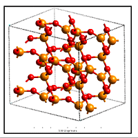
 Structures,
energetics and charging behavior of all defects related to
oxygen vacancies, hydrogen and their complexes in silica
have been investigated. The charging behavior of the
defects provides insight into the tunneling processes
related to stress induced leakage current, which is
considered a forerunner of dielectric breakdown.
Structures,
energetics and charging behavior of all defects related to
oxygen vacancies, hydrogen and their complexes in silica
have been investigated. The charging behavior of the
defects provides insight into the tunneling processes
related to stress induced leakage current, which is
considered a forerunner of dielectric breakdown.
Let us consider the two-step tunneling of an electron onto a defect and from the defect into the kathode. Typically, such a tunneling process has a higher transition rate than the direct tunneling through the oxide, which is a result of the exponential decay of the wave function in the oxide band gap.
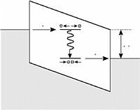 The figure on
the left illustrates the schematic energy level diagram as
function a spacial coordinate running through a
metal-oxide semiconductor structure. The shaded area
indicates filled electron states. The oxide band gap is
tilted due to an applied voltage. An electron enters a
defect level in the oxide band gap. In response the defect
distorts the rather flexible silica framework and places
the level at lower energy. The electron is trapped unless
the voltage is sufficiently high that the electron can
tunnel into an unoccupied state of the cathode.
The figure on
the left illustrates the schematic energy level diagram as
function a spacial coordinate running through a
metal-oxide semiconductor structure. The shaded area
indicates filled electron states. The oxide band gap is
tilted due to an applied voltage. An electron enters a
defect level in the oxide band gap. In response the defect
distorts the rather flexible silica framework and places
the level at lower energy. The electron is trapped unless
the voltage is sufficiently high that the electron can
tunnel into an unoccupied state of the cathode.
This principle allows to differentiate defects according to their ability to carry a leakage current. When a defect in silica is charged, new bonds are formed and old ones are destroyed. The shifts of the defect levels are typically so large that most defects trap electrons. This may be the ultimate reason for silica being such a good insulator. Only two hydrogen complexes with sufficiently small relaxations to contribute to the leakage current have been identified.
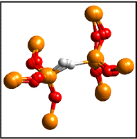 The
figure on the left shows the overlayed structure of the
hydrogen bridge in silica in positive,neutral and negative
charge states. In this defect a hydrogen is inserted into
an oxygen vacancy. The small relaxations upon changing its
charge make this defect the prime candidate for carrying
the stress-induced leakage current.
The
figure on the left shows the overlayed structure of the
hydrogen bridge in silica in positive,neutral and negative
charge states. In this defect a hydrogen is inserted into
an oxygen vacancy. The small relaxations upon changing its
charge make this defect the prime candidate for carrying
the stress-induced leakage current.
The calculated energy loss during the inelastic tunneling via the defect of 1.7 eV is in perfect agreement with experimental results 1.5 eV. Electrically detected magentic resonance (EDMR) spectra can be interpreted as superposition of the spectra of the two defects we predicted
For further details see
- "Hydrogen Electrochemistry and Stress-Induced Leakage
Current in Silica",
P.E. Blöchl and J. Stathis, Phys. Rev. Lett. 83, 372 (1999). - "First-Principles Calculations of Defects in
Oxygen-Deficient Silica Exposed to Hydrogen",
P.E. Blöchl, Phys. Rev. B 62, 6158 (2000). - "Aspects of Defects in Silica Related to Dielectric
Breakdown of Gate Oxides in MOSFETs",
P.E. Blöchl, and J.H. Stathis, Physics B 273-274,1022 (1999).